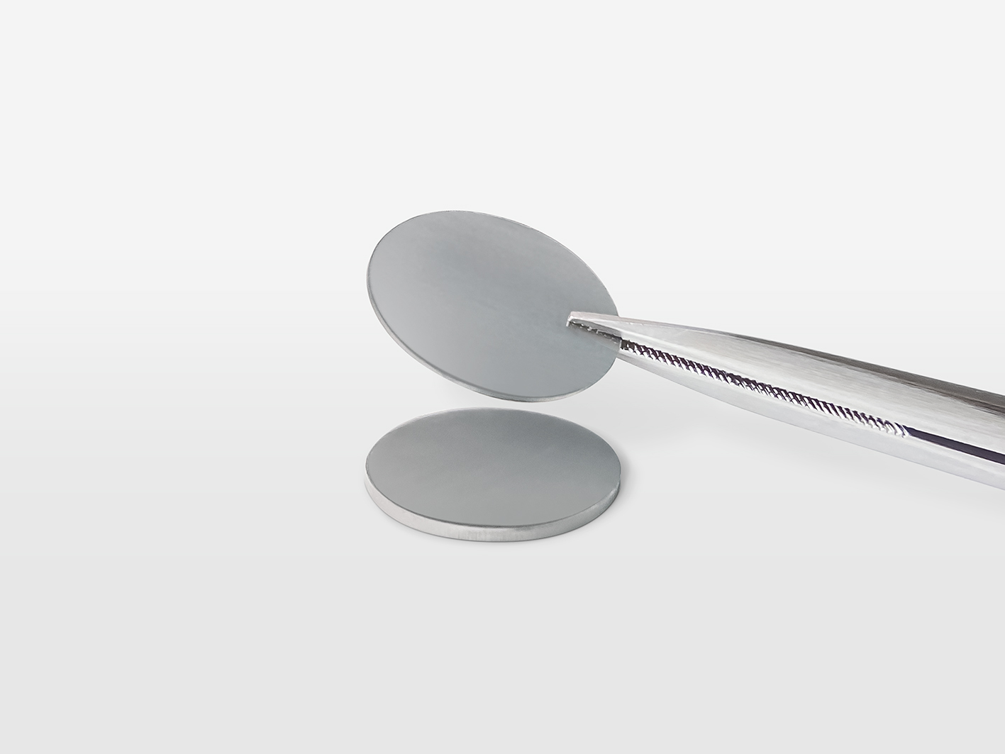
Newly Developed KABRA® Process that Achieves Large-Diameter Diamond Wafer Manufacturing
DISCO CORPORATION, a semiconductor manufacturing equipment manufacturer (Head Office: Ota-ku, Tokyo; President: Kazuma Sekiya), has developed a process for diamond wafer manufacturing that applies the KABRA process, an ingot slicing method using laser technology. This process contributes to increasing the diameter of diamond wafers.

Developmental Background
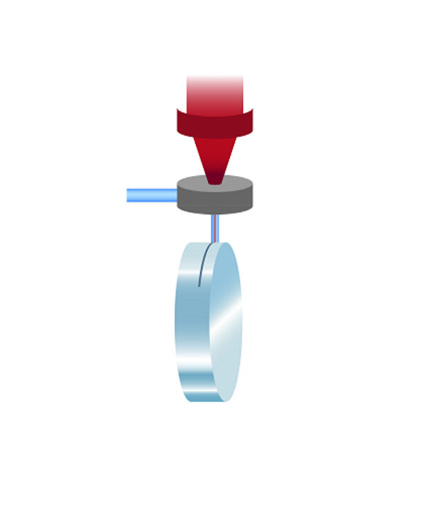
Diamond is often called the “ultimate semiconductor material” due to its superior material characteristics compared to Si, SiC, and GaN. In particular, as diamond has excellent insulation strength and heat conductivity, it is expected to be a good material for power semiconductors, and device development is underway at various research institutes. On the other hand, as it is an extraordinarily hard material, it came to be known that it is difficult to process mechanically. Therefore, laser became the general method used to slice wafers from a diamond crystalline ingot. However, with the conventional laser slicing method, as the ingot is processed from the sidewall, there was a limitation on the ingot diameter, and it was difficult to increase it. With KABRA slicing, there is no limitation on the ingot diameter as the laser is irradiated from the upper surface of the ingot, making it possible to increase the ingot diameter.

Figure 1: Conventional slicing method using laser

Figure 2: KABRA for diamond processing
Features
- Supports large-diameter ingots exceeding Φ50 mm
With the conventional method where the laser is irradiated from the sidewall of an ingot (Figure 1), the largest supported diameter was approx. Φ30 mm, but with the KABRA method (Figure 2), as the laser is irradiated from the upper surface of the ingot, there is no limitation on the ingot diameter. - Splitting wafers with a thickness of 100 µm or less is possible
By irradiating the laser at a shallow depth from the upper surface of the ingot, it is possible to split thin wafers. Therefore, a larger number of split wafers can be expected compared to the conventional method. - Achieves equivalent or higher throughput compared to the conventional method
The splitting speed is equal to or faster than the conventional method, achieving lower processing costs.
In addition, 45 patents related to this technology have been registered.
Future Schedule
Test cuts are available. Please contact a DISCO sales representative.
About DISCO
DISCO is a semiconductor equipment manufacturer that provides precision processing equipment, including dicing saws and grinders, and precision processing tools (blades and wheels) used for manufacturing semiconductors and electronic components. In addition to these products, as a result of pursuing optimal processing results for customers through the provision of the technology used with the equipment and tools, DISCO products and processing technologies have been widely adopted by device manufacturers and semiconductor subcontractors both domestically and internationally. For details, please visit the DISCO website at www.disco.co.jp.
Contact
Please feel free to contact us with any questions or inquiries.
