KABRA!zen*1Developed:
Full-Automatization of KABRA®*2*3Laser Slicing Technology
DISCO CORPORATION (Head Office: Ota-ku, Tokyo; President: Kazuma Sekiya) has developed KABRA!zen, which achieves the full-automatization of the KABRA process: an ingot slicing method which uses a laser. This equipment enables a series of processes required in the KABRA process, including laser irradiation, wafer separation, fine grinding down to the designated thickness, and grinding of the top surface of the ingot, all unmanned, further accelerating advances in the efficiency of SiC wafer production. KABRA!zen will be exhibited in SEMICON Japan, held at Tokyo Big Sight from December 13 to 15. DISCO has already received inquiries from major wafer manufacturing companies and is aiming to ship test equipment within 2018.
*1 Trademark pending
*2 Total no. of acquired and pending patents: 53 (as of December 11, 2017)
Registered trademark (Registration No. 5850324)
*3 An ingot slicing method in which a separation layer (KABRA layer) is formed at a specified depth by continuously irradiating an ingot with a laser, producing wafers starting from the KABRA layer. KABRA stands for Key
Amorphous-Black Repetitive Absorption. For details, please visit the KABRA
process site.
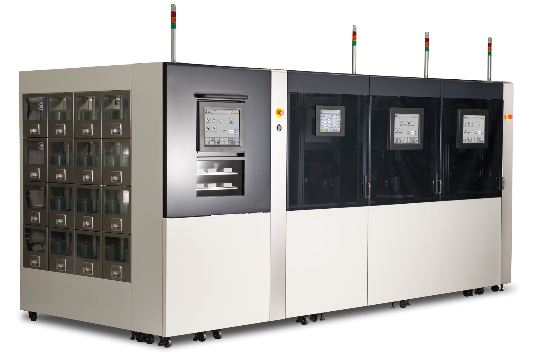
(Equipment configuration when performing the KABRA process using the minimum amount of equipment)
Development Background
Because the existing KABRA process requires an operator to remount workpieces before each process (including laser irradiation, wafer separation, fine grinding down to the designated thickness, and grinding of the top surface of the ingot), the throughput was affected by the ability of the operator. Furthermore, it is predicted that there will be an increase in electric power consumption across a wide range of products due to the development of the IoT and the use of electronics in vehicles, and there are expectations for the widespread use of energy-saving power devices which use next generation-materials, such as SiC. However, in the conventional diamond wire saw ingot slicing method, a low throughput and a large amount of material loss during processing was causing an increase in manufacturing costs.
Advantages of KABRA!zen
Fully-automatic transfer between processes achieves approx. 50% increase in
throughput
The throughput has been drastically improved through the full-automatization of transfers between each
process: laser irradiation, wafer separation, fine grinding down to the designated thickness, and grinding
of the top surface of the ingot.
Customization of the number of connected machines
Because the system joins each of the laser, separation, and grinding processes, the number of machines
used for each process can be customized according to the various criteria, such as the number of wafers
produced, surface finish condition, etc.
Full-automatization possible through retrofit
Even if you are currently using the preceding, manual KABRA equipment, full-automatization of
your existing equipment is possible through a retrofit.
The fully-automatic process and all equipment used in the KABRA!zen process (to be exhibited at SEMICON
Japan 2017) are developed by DISCO.
Number of Related Patents: 53 *Including pending patents (as of December 11,
2017)
Breakdown: 13 process-related patents, 3 full-automatization (KABRA!zen) patents, 19 laser irradiation
patents, 7 separation patents, 2 grinding patents, 9 miscellaneous patents
Reference
The equipment was designed assuming full auto mass production for SiC Epi Ready wafers*4using KABRA!zen. (E.g.)
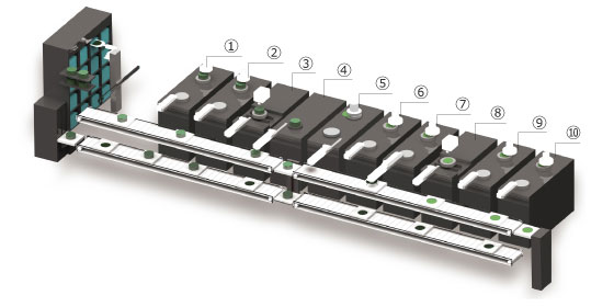
①Ingot coarse grinding
②Ingot fine grinding
③Laser irradiation
④Wafer separation
⑤Wafer edge trimming
⑥Wafer coarse grinding
⑦Wafer fine grinding
⑧Laser marking
⑨Wafer polishing (Both sides)
⑩Wafer fine polishing (Si surface)
*4:Wafers polished to high quality before thin film crystals are grown (epitaxial growth) on the surface. Because crystal defects generated during ingot growth may affect device characteristics, it is necessary to grow a thin crystal layer (epi layer) without defects on the wafer surface.
Future Schedule
| December 13–15, 2017 | SEMICON Japan 2017 (reference exhibit) |
|---|
Contact
Please feel free to contact us with any questions or inquiries.